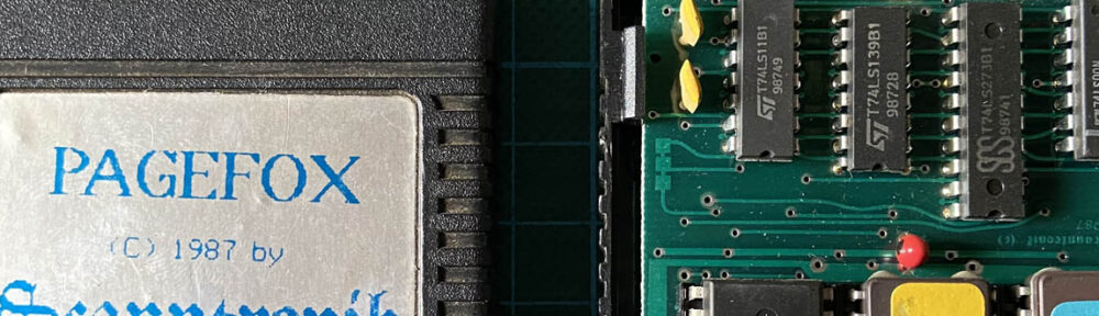
Pagefox is a DTP (desktop publishing) software that comes as a cartridge for the expansion port of the Commodore 64. It was developed by Hans Haberl — who also created the graphics editor Hi-Eddi and the word processor Printfox — and it was published and sold by the small German company Scanntronik which is actually still in business today.
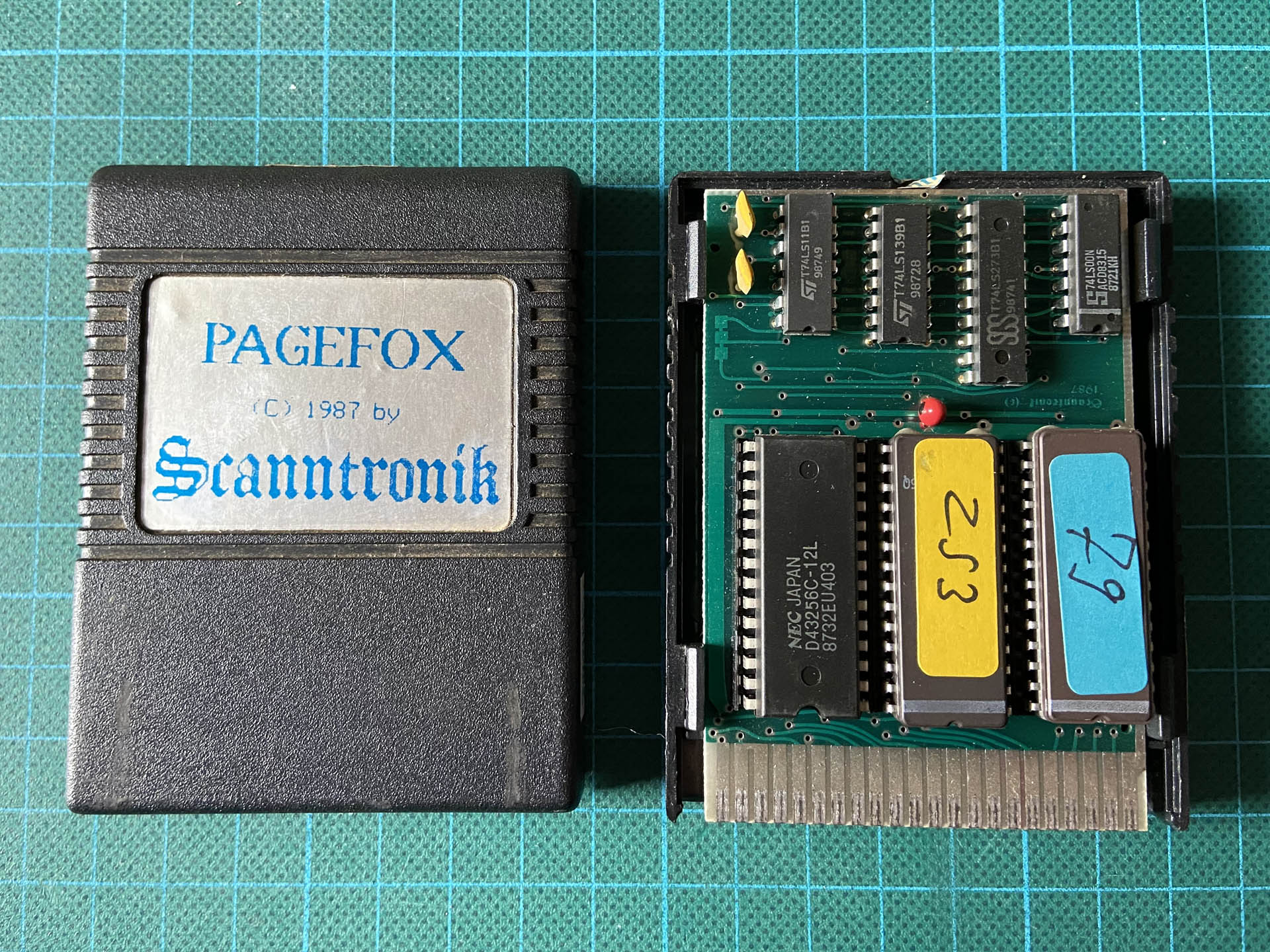
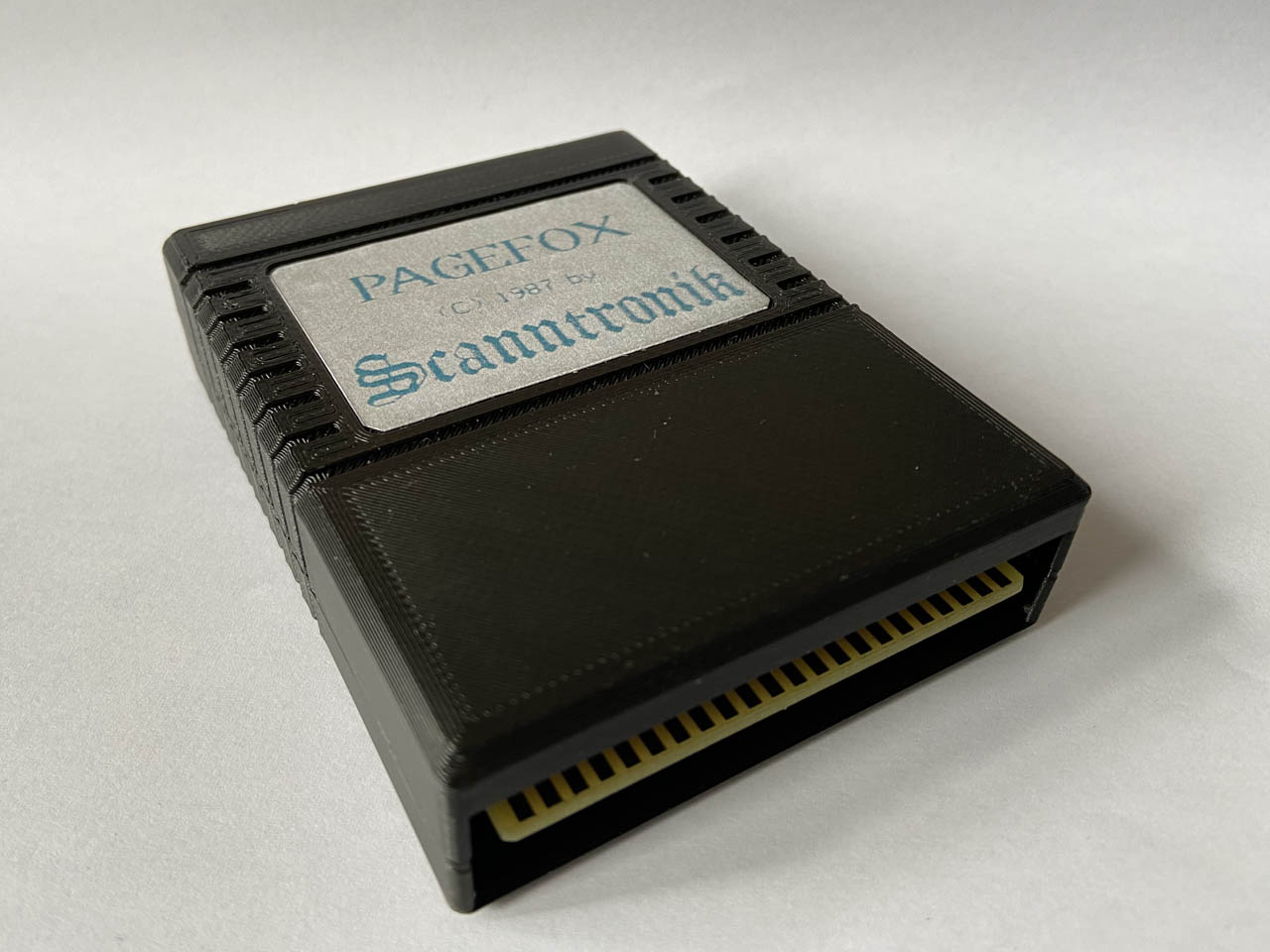
Pagefox cartridge pried open
Primitive by today’s standards of course, it was quite sophisticated when it was released in 1987. The Pagefox cartridge features two 32k ROMs holding the Pagefox software, additional 32k of RAM, and a bank-switching logic to make all of that usable on the C64. Back then as a kid, I would have loved to have one of those cartridges but there as no way I could afford it.
The Project
Today, even with prices for vintage hardware on a steep rise, the cartridge can be found occasionally for a very reasonable amount of money. A couple of months ago, I was able to pick one up myself. Of course, there was no way I was actually going to use this for its original purpose these days. So I thought it might be a nice project to reverse engineer the cart and see if I could replicated it.
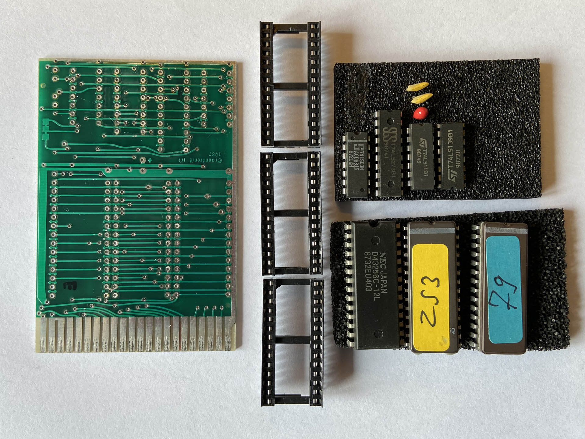
PCB stripped of all components
I did a quick research and it seemed that this hadn’t been properly done before, so why not! Later on, when most of my work was already done, I found out that Frank Reichel and Jens Schönfeld had already reversed Pagefox in 2011 and had partially published their findings on Forum64. Good thing that I missed that at first or I might have missed out on a nice and fun little project. 🙂
Preparations
Anyway, the first steps were opening the cartridge case (which was surprisingly hard to do without damaging it) and desoldering all components from the PCB. I used my ZD-915 station for the latter, which is a great help for someone like me who is lacking the necessary desoldering skills.
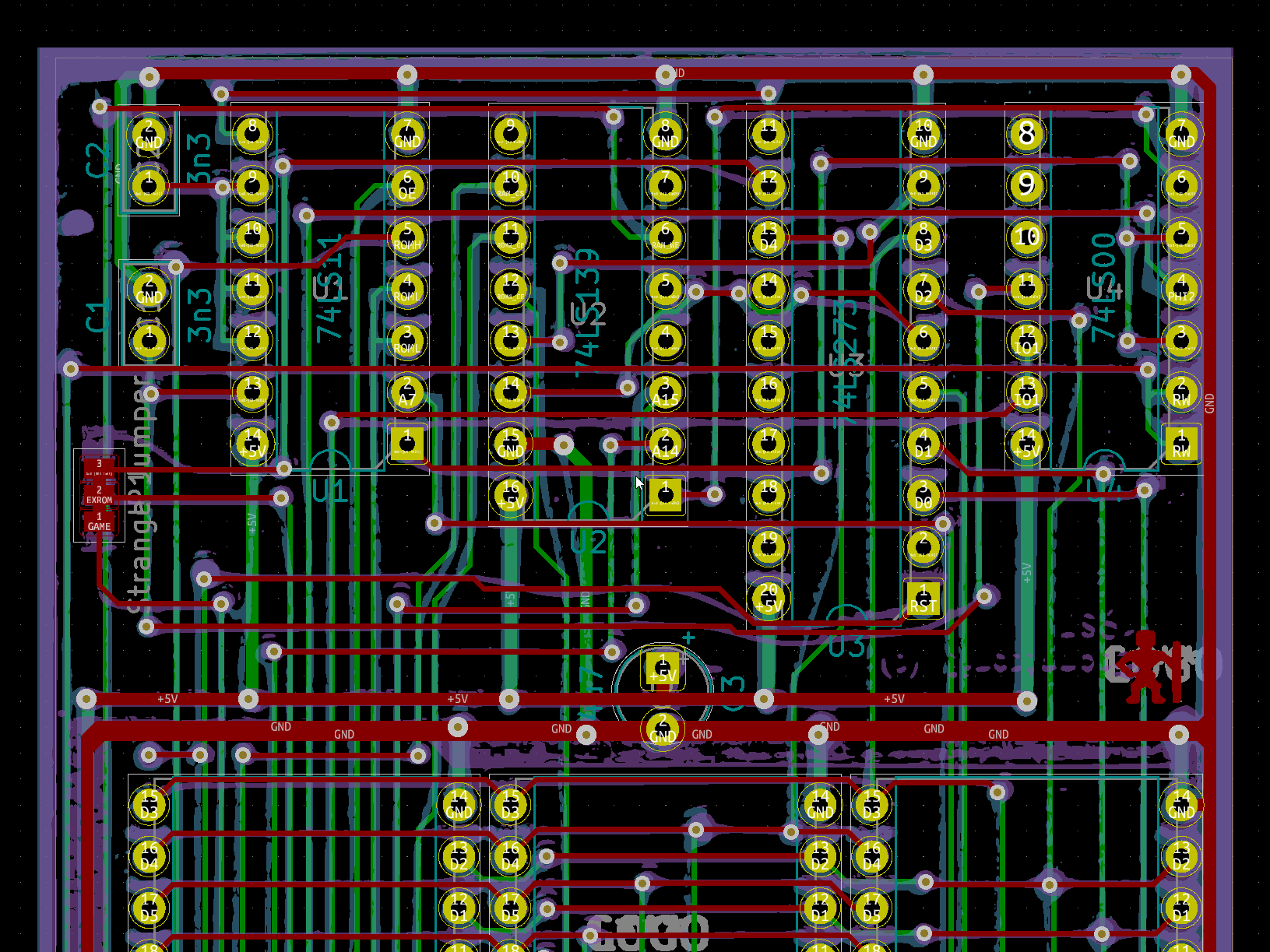
Using scanned images as reference in PCBnew
Then I put both sides of the empty and cleaned PCB on a flat bed scanner to get good images of the board layout. There are some CAD tools out there which allow such images to be placed directly below the new board layout for reference. But I was going to use the KiCAD tools for the job because that is what I know how to use somewhat. Unfortunately, KiCAD is still lacking that feature so I needed to do some post-processing of the scans.
I mirrored the image of the bottom side, did some manual cleaning, increased contrast by a lot, and converted to black & white. Then I used the “Bitmap to Component Converter” that comes with KiCAD to create a “component” for each side of the PCB, placing the top side on the Eco1.User layer and the bottom side on the Eco2.User layer.
Working with KiCAD
The first thing I did after creating a new project in KiCAD was to add all the components I found on the original PCB to the schematic:
| 1 | 74LS11 | U1 | Triple 3-input AND gate |
| 1 | 74LS139 | U2 | Dual 2-bit demultiplexer |
| 1 | 74LS273 | U3 | Octal d-type flip-flop |
| 1 | 74LS00 | U4 | Quad 2-input NAND gate |
| 1 | D43256C-12L | U5 | 32k x 8 SRAM (used HM62256) |
| 2 | NMC27C256 | U6,U7 | 32k x 8 EPROM |
| 2 | 3.3nF | C1,C2 | Ceramic caps |
| 1 | 4.7µF | C3 | Tantalum capacitor (used electrolytic) |
| 1 | CN1 | Board edge connector to expansion port |
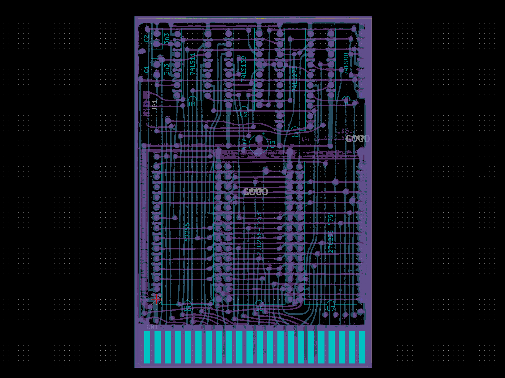
Without any connections between the components for now, I then exported the net list and switched over to PCBnew (like you do in KiCAD). There, I added the two pseudo-components containing the scanned images of the original traces, aligned them, and placed all the actual components where they belong.
Replicated traces pin by pin
Basically the only thing left to do now was to trace the connections on the original PCB. A good point to start was the edge connector because the purpose of most pins is very clearly defined there. So, I started by assigning net labels in the schematic to all connector pins that were used on the original PCB and by marking the remaining ones as not connected. Then I picked one of the pins, visually traced its connections to other pins in PCBnew, and assigned the same net label to those. Exported/imported the net list and then actually routed the track, trying to follow the original one on the scanned image.
The next few hours were spent going back and forth between the schematic and the board layout countless times, tracing all connections carefully until every pin of each component in the schematic was either connected or explicitly marked as not connected.
Ready for a Prototype
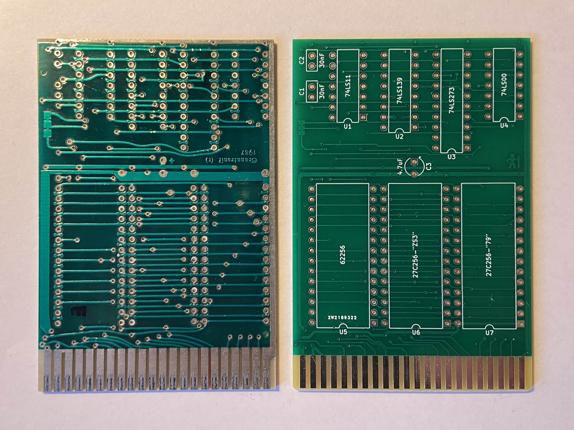
Original board and its replica
When finally all electrical and design rule checks in KiCAD passed, I felt confident enough to order a prototype batch of the resulting board. I used AllPCB this time, because they are currently giving away one free prototype coupon to each customer per month. This offer includes 5 PCBs and free express shipping around the world.
So, only six days later I received the package containing the first revision of my newly created Pagefox board. I assembled one of the boards, pushed the ICs from the original cartridge into the sockets, inserted the cartridge into a C64, switched it on — and got just a black screen.
Bug Fixing
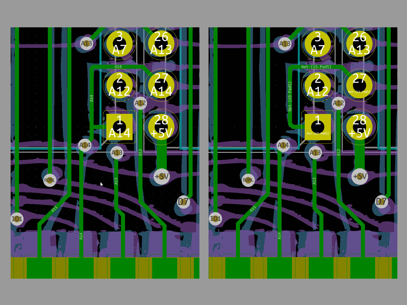
Corrected the routing of the A14 signal (before / after)
This was a little disappointing, but then again, maybe it would have been to easy if it had worked on the first try. So, I went back to double check all the connections using the continuity tester of my multimeter. It really helped at this point, that I had not only traced the original board layout but also reconstructed the validated schematics. About an hour later I noticed that I had incorrectly routed the A14 signal!
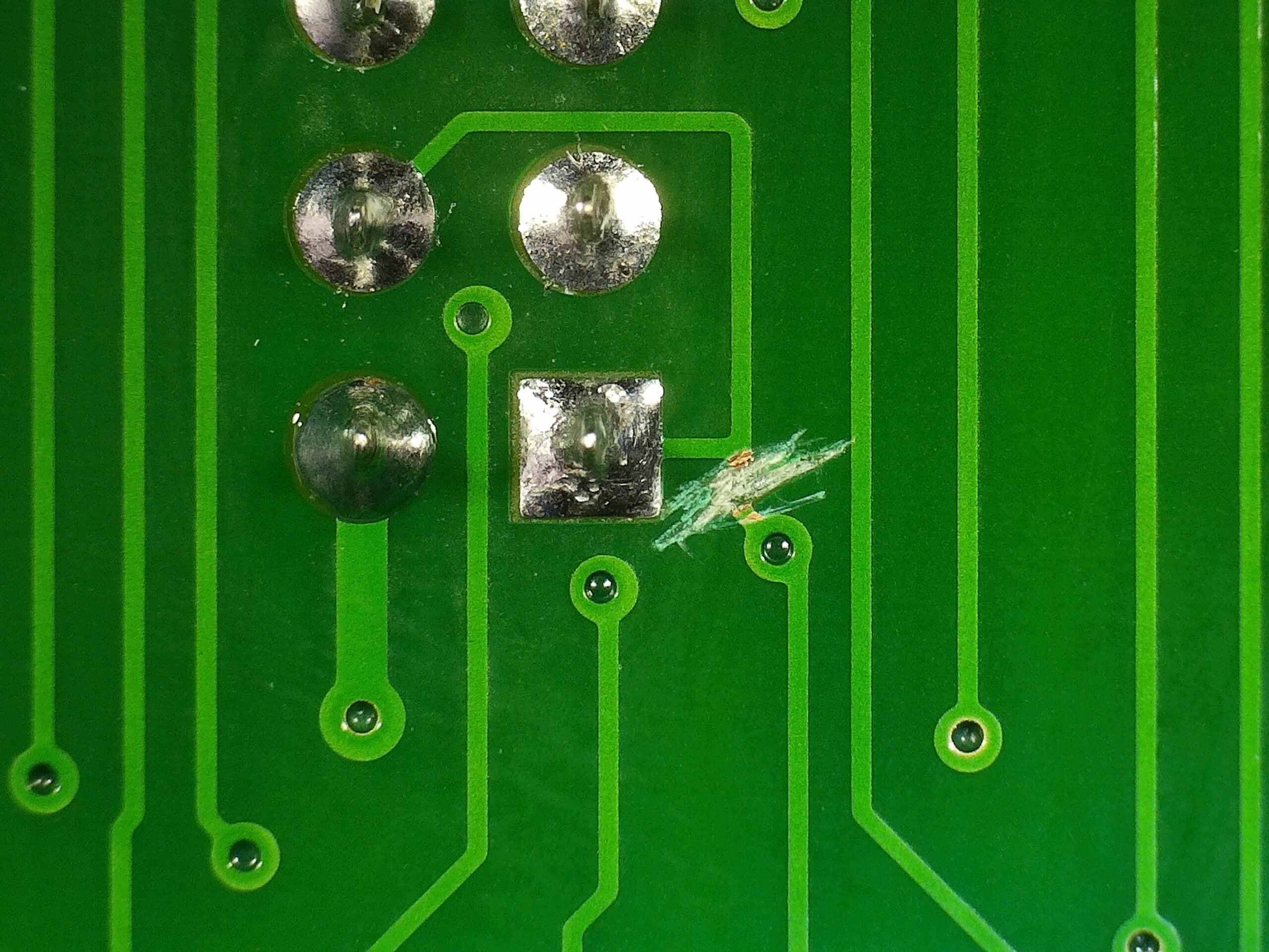
Fixed the PCB by cutting the right trace
After fixing the schematics and board layout in KiCAD, I located and cut the trace on the PCB and tried again:
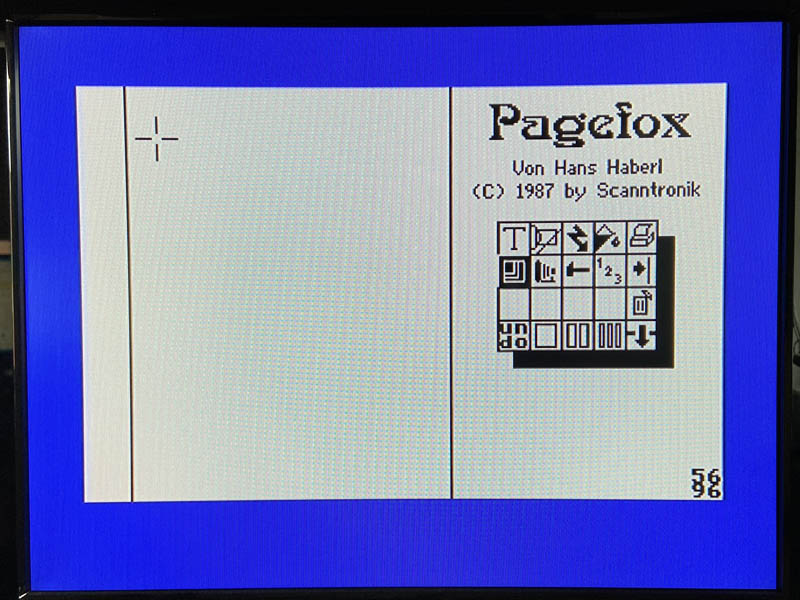
Pagefox running off the replicated PCB
Finalizing
The cartridge seems to be working now! To complete the replication, I inserted all new ICs into the sockets, using two W27C512 EEPROMs which are cheaper and easier to handle these days than their original counterparts, and a HM62256 SRAM that I had at hand.
Finally, I adopted the 3D model of a cartridge case that I had created for the “Magic Formel” cartridge a while back to fit the Pagefox PCB. Maybe later I’ll also find some kind of silvery label to properly replicate the original. For now, a simple photocopy on plain paper will have to do:
The finished replica
Looking back, it would have payed off for me to take more care when preparing the scans of the original PCB. I suspect that I could have avoided the error I made routing A14 that way. But, all in all it was a fun project and I’m satisfied with the result.
I hope you will understand that this is one of the cases where I cannot share the entire project. I could not and would not do so without the permission of the copyright holders. For now you’ll find here the schematics that I produced, since these have been essentially published before, as mentioned above.


Pingback: C128 Diagnostic Cartridge #325093-01 Replicated | hackup.net