The Idea
Recently, I’ve been repairing a few broken and slightly weathered motherboards for Commodore C16 and Plus/4 computers.
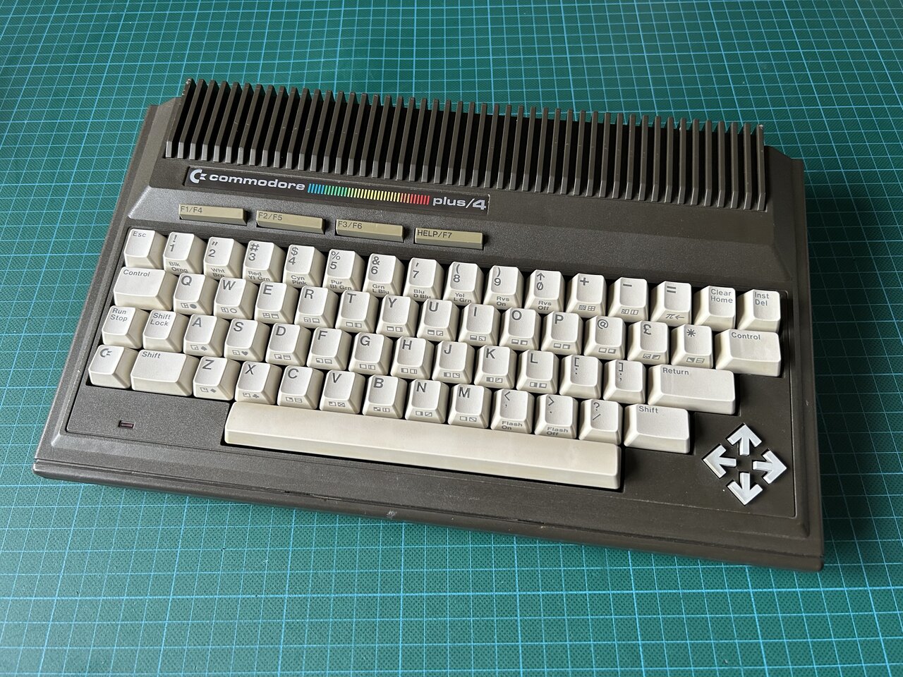
Despite its stylish design, the Plus/4 was no success for Commodore.
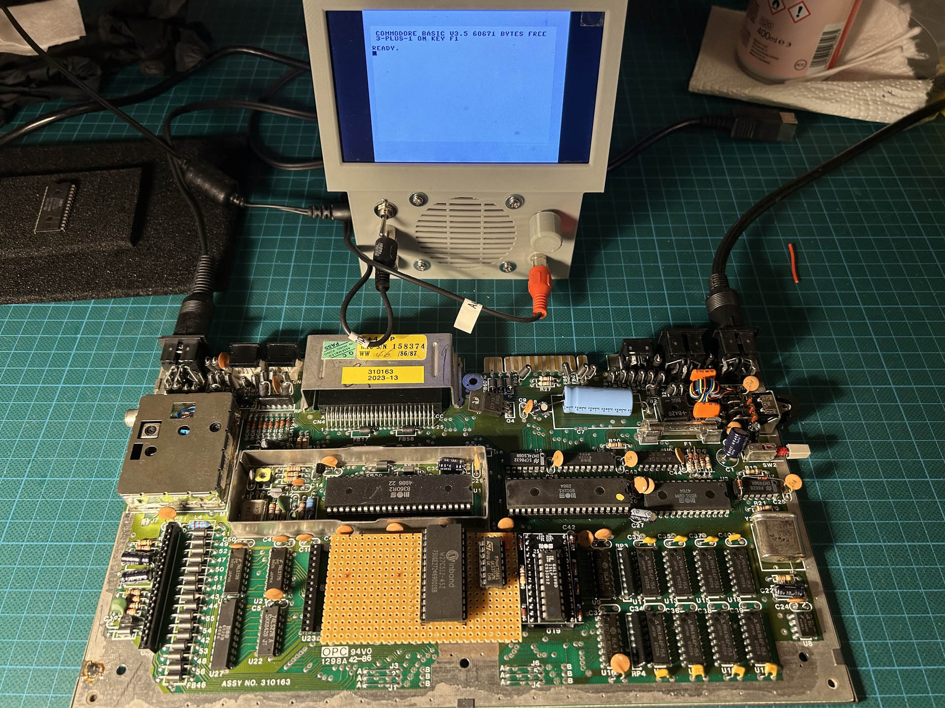
When I ran out of spare parts, I replaced the defective Kernal ROM on one of the Plus/4 boards with a W27C512 EEPROM. You can still source a used W27C512 easily and somewhat cheaply (on eBay, for example), making it my all-purpose tool for replacing ancient parallel ROMs.
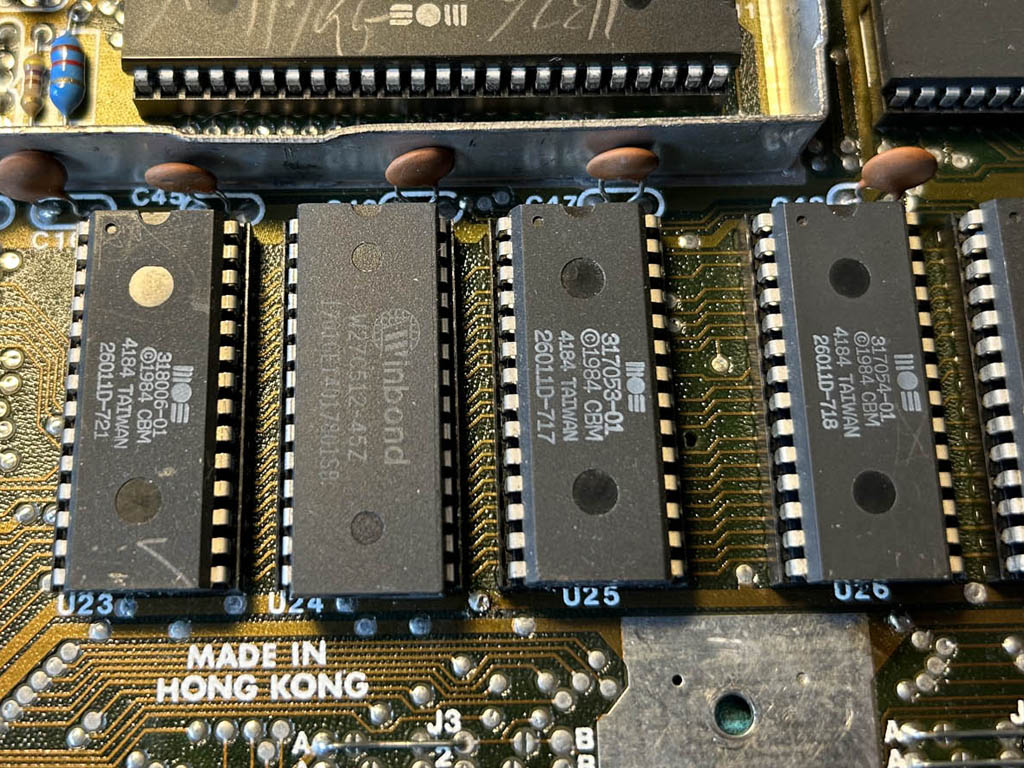
The four ROM slots U23-U26 on a Plus/4 board (left to right: Basic, Kernal, Function low, and high). The Kernal already replaced with a W27C512.
It worked fine in this case as well: All I had to do was write the 16k ROM image to the EEPROM four times in a row to fill its 64k of memory. And I had to add a small piece of jumper wire to connect pin 1 of the ROM socket to ground, since it is dangling on the Plus/4 board, which would not work for A15 on the EEPROM.
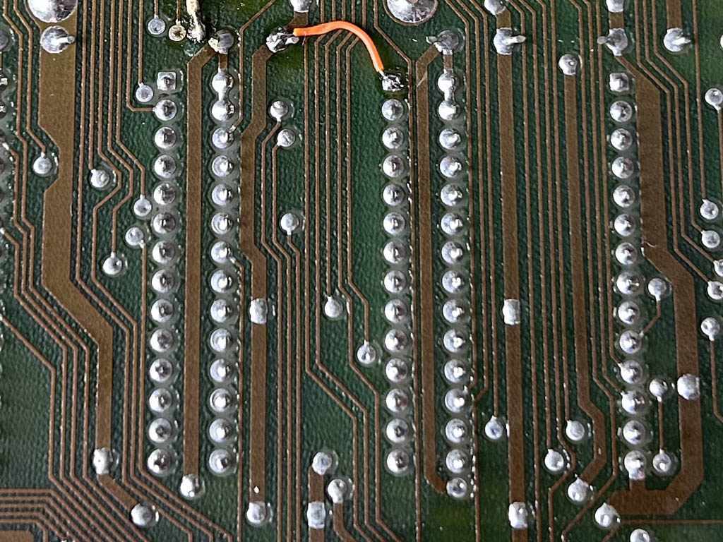
Bodge wire tying pin 1 of the Kernal socket to GND.
It worked fine, but it still felt a little wasteful. After all, the W27C512 with its 64k of memory could theoretically replace all four ROM chips sitting next to each other. This would be all the more useful since these ICs seem to always be socketed in the Plus/4.
The Theory
The tricky part would be to properly encode the four separate /CS signals. They had to select one of the 16k memory banks instead of the original IC. Designing a simple logic to do this sounded like an interesting puzzle to me.
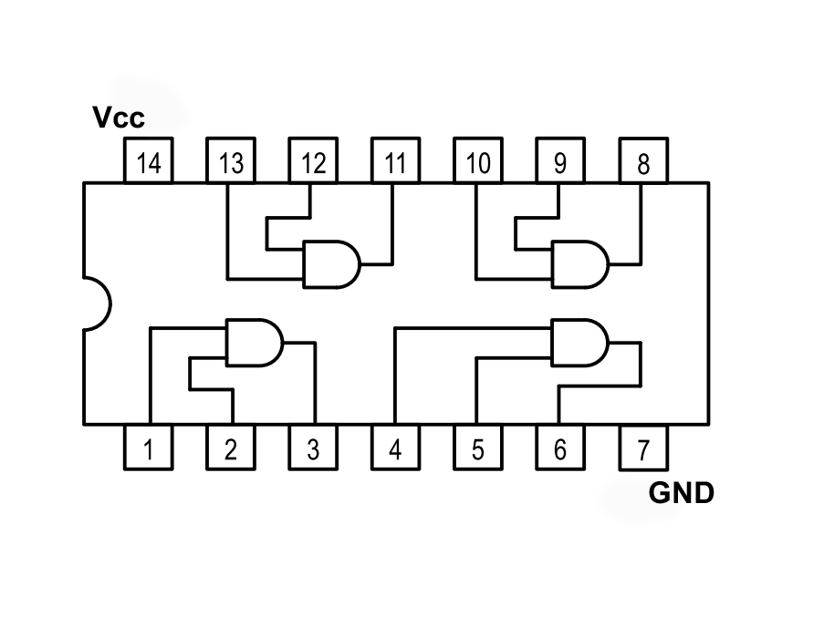
It took detours across different types of logic gates for me to realize that the obvious solution is to simply use AND gates as provided by this 74LS08 chip.
It might have been an easy task for others, but I hadn’t tried anything like this before. So it actually took me quite a while and a few detours through different types types of logic gates.
In total there are five different states to consider:
1. no ROM IC selected
2. U23 selected
3. U24 selected
4. U25 selected
5. U26 selected
And there are four input variables that describe these states:
                   Y1 Y2 Y3 Y4
1. none selected   1  1  1  1
2.  U23 selected   0  1  1  1
3.  U24 selected   1  0  1  1
4.  U25 selected   1  1  0  1
5.  U26 selected   1  1  1  0
The values of the four variables Y1-Y4 are the chip select signals of U23-U26. At any given point in time, no more than one of the ROM chips is selected by pulling the /CS pin of that chip low. When the CPU is not reading from any of the ROMs, all four lines are high.
From these inputs, the following values must be derived for A14, A15, and /CS of the 64k EEPROM:
                   Y1 Y2 Y3 Y4    A15 A14    /CS
1. none selected   1  1  1  1     0   0      1
2.  U23 selected   0  1  1  1     0   0      0
3.  U24 selected   1  0  1  1     0   1      0
4.  U25 selected   1  1  0  1     1   0      0
5.  U26 selected   1  1  1  0     1   1      0
As it turns out, this can be done with only four 2-input AND gates:
A14  =  Y1 & Y3
A15  =  Y1 & Y2
/CS  =  Y1 & Y2 & Y3 & Y4  =  A15 & Y3 & Y4
Bottom line: A single 74LS08 logic IC should do the job!
The Prototype
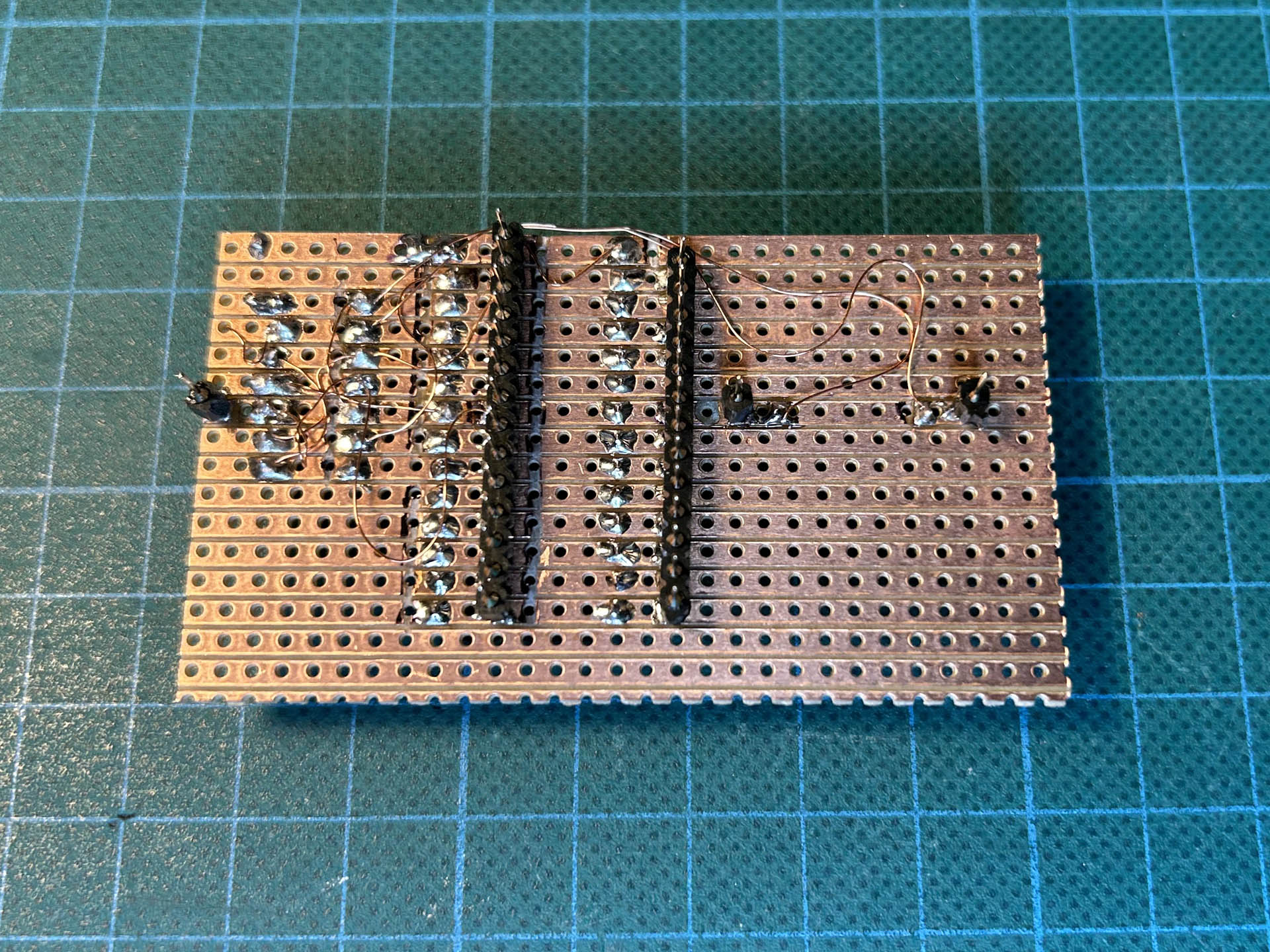
The not so pretty wiring of the prototype.
Once I had that sorted out, I was very curious to see if it would actually work. So, I grabbed a piece of perf board, a couple of DIP sockets, and some wire to build a proof of concept.
Yay! We have a working prototype!
When I had finished the the ugly business of wiring up the prototype I plugged it into the sockets of a Plus/4 board and was delighted to find that it worked like a charm!
The remaining problem with this solution was that it would not fit into the case of the computer. In a Commodore Plus/4, there is probably no more than a few millimeters of free space between the top of the socketed ROMs and the bottom of the keyboard. My first idea was to rotate the EEPROM by 90 degrees and to move it as close as possible to the tin box that houses the TED.
Making it fit

There is very little room between the ROMs and the keyboard when the case of the Plus/4 is closed.
But even if that would fit, it would not make for a nice solution, so I started searching the web to see what tricks others might have up their sleeves when it came to fitting such contraptions into a Plus/4.
It was at this point that my own pride in my latest idea was slightly dampened: I found out that I wasn’t the first to come up with the idea of replacing those four ROMs with a single one. Kudos to MCes, a member of the Plus/4 World Forum, for beating me to the punch by at least a few years! His solution, called the “Low Power Plus4 ROMset”, also uses but a single logic IC. Although I cannot make it out on the pictures, I am guessing that it is a 74LS08 as well.
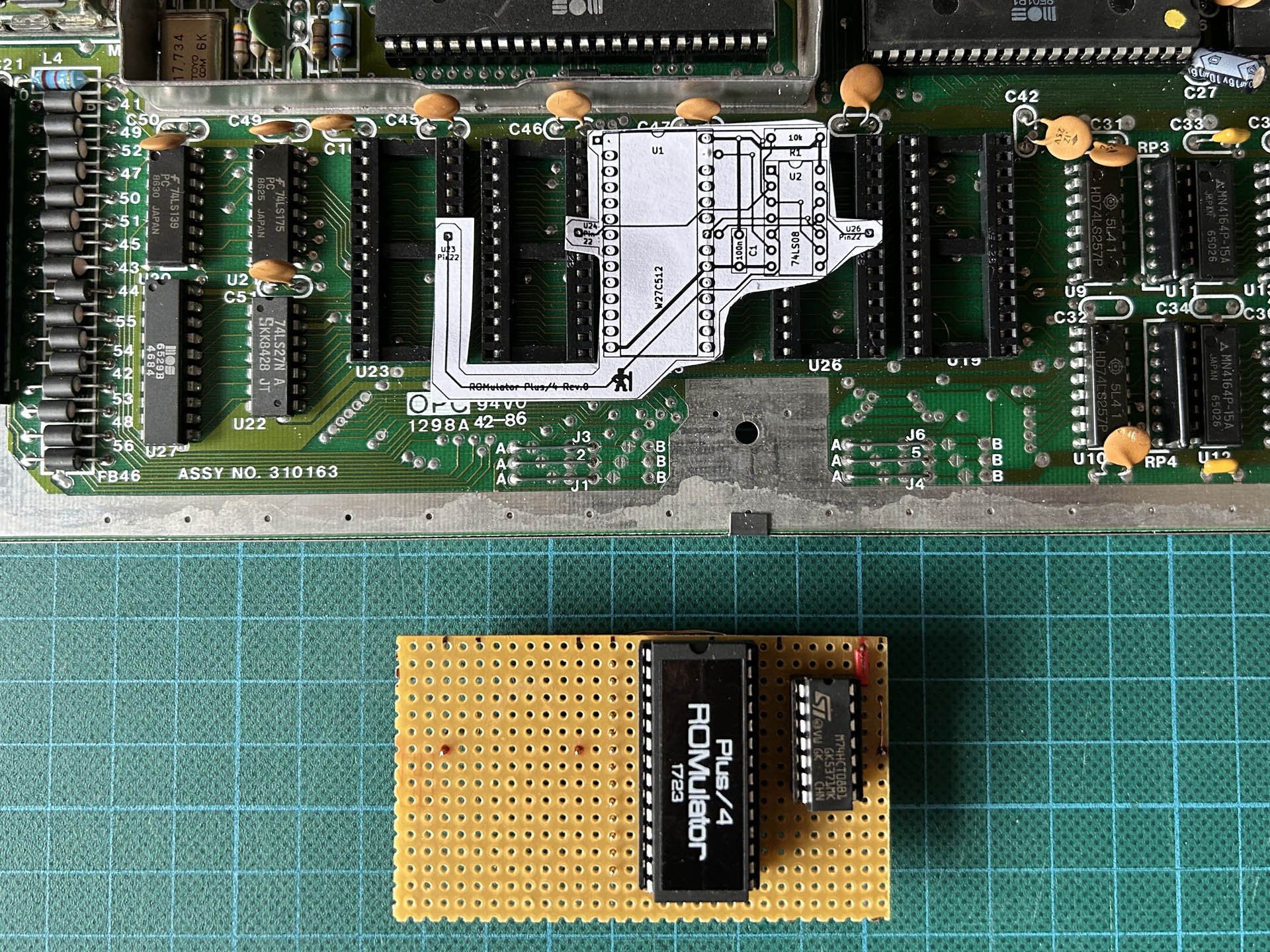
First draft for a PCB that might fit into the case of the Plus/4.
Oh, well. I suppose it gets harder to come up with unique new ideas for ancient computers every decade. But I had come too far to stop there, and I still wanted to make my on version of this topic, which I had by then given the working title “ROMulator Plus/4”. The Low Power ROMset showed two ideas that I decided to borrow from:
- Plug the EEPROM through a thin PCB directly into the socket on the motherboard to save height.
- Route the /CS signal from the Basic ROM around the Kernal ROM to still allow for the use of a separate Kernal replacement.
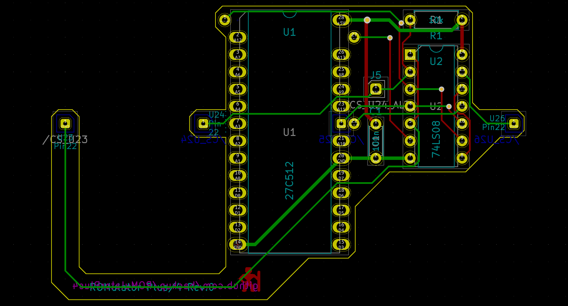
KiCAD layout of the ROMulator Rev.0
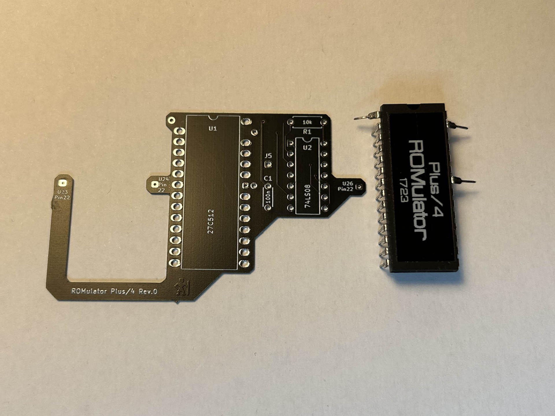
As usual, I used KiCAD to layout the PCB. Since I wanted to plug the EEPROM through the PCB into the socket, I ordered the PCBs with a thickness of 0.8mm instead of the usual 1.6mm.
Assembly and tests
A couple of weeks later, the PCBs for the first revision of the ROMulator were delivered to my door. Eager to see if everything would work out, I sat down to assemble the first unit. But there were a few things to consider: Both ICs had to be soldered directly to the board. The pins of the logic IC had to be trimmed carefully, while the pins of the EEPROM had to be left as long as possible to find a good hold in the socket. Then three of these legs had to be bent so that they would not reach into the socket.
Getting read to assemble the first unit.
Soldering the four single pin headers for the /CS lines to the bottom of the board was by far the hardest part. I managed to rip off one of the solder pads in the process but fortunately I was able to patch it again.
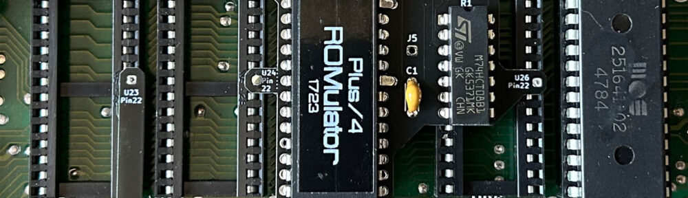
When I plugged the finished ROMulator into the Plus/4 test board I was happy to find that everything fit. It even made good enough contact with the ROM sockets. And most important: The Commodore Plus/4 still seemed to work fine!
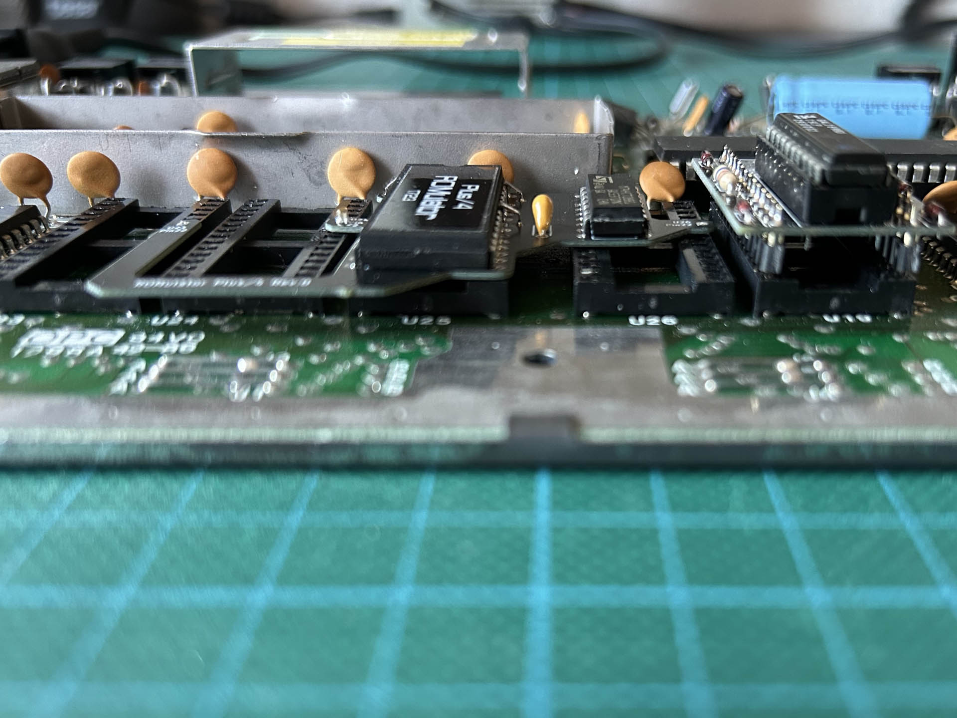
The ROMulator fits tightly into the ROM sockets.
Finally, I tried the assembled and tested unit in the only Plus/4 I own that actually has a complete case, to see if it would fit in there. No problem at all!
PROSPECTS
Still, there are a few things I plan to change in the next revision of the ROMulator:
- Make the four /CS pads a little bigger, hoping to make them more resistant to extensive soldering.
- Move the 74LS08 100mil closer to the EEPROM so that there is more distance between its pins and the empty socket below it.
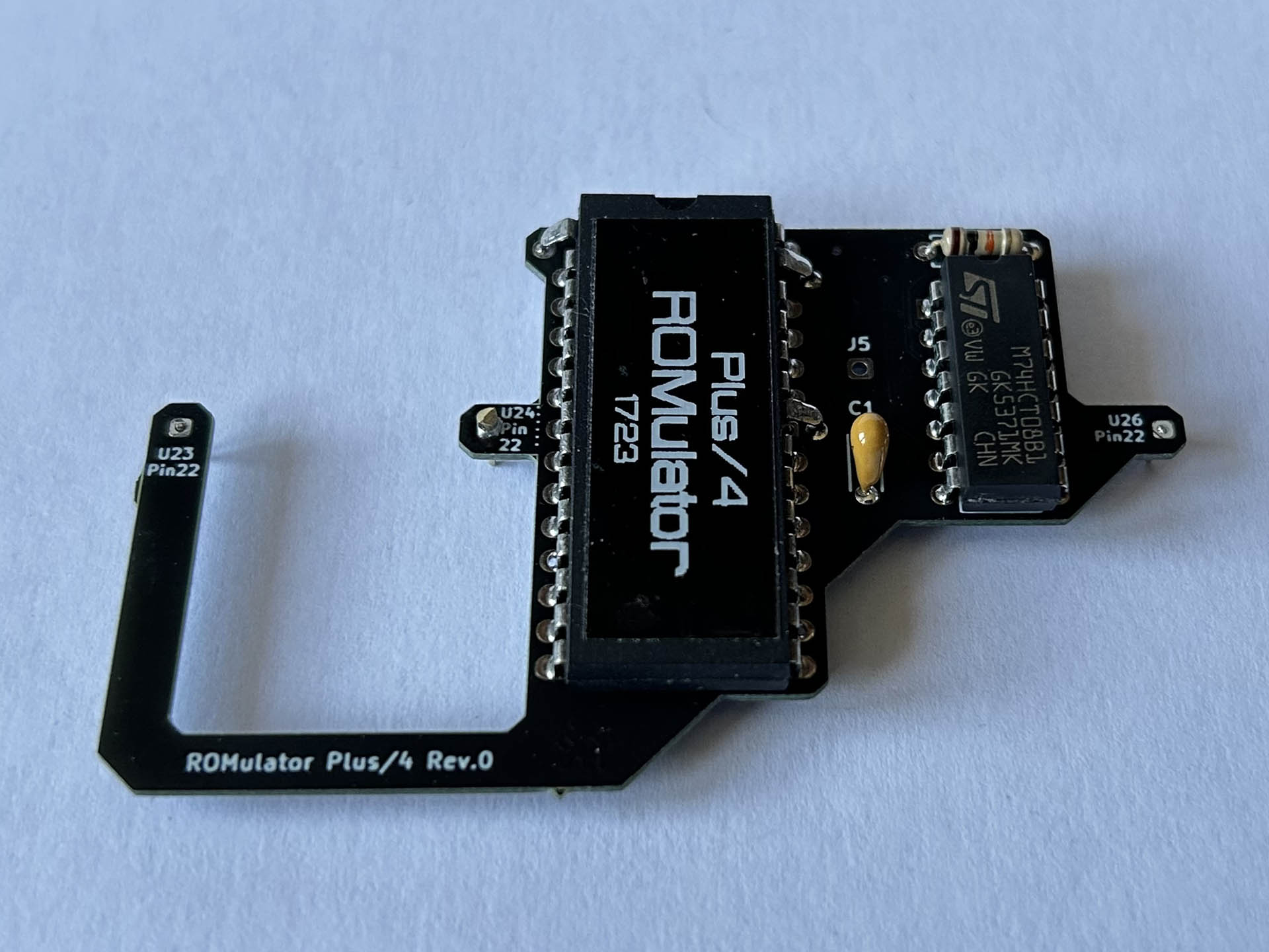
The first unit assembled and tested.
When this is done and everything else is cleaned up, I will share my project files as I do most of the time. But first, there is one more small project in the queue: The attentive reader may have noticed that the PLA replacement in the pictures doesn’t fit into the Plus/4’s case either. Let’s see what we can do about that…


Pingback: How to Lower Your PLA: The PLA264 | hackup.net
Pingback: Making Cartridges for the Commodore C16, C116, and Plus/4