In my previous post I described in detail how I created a ROM replacement for the Commodore Plus/4 computer and how I made sure that it would fit into the very tight space of the closed case.
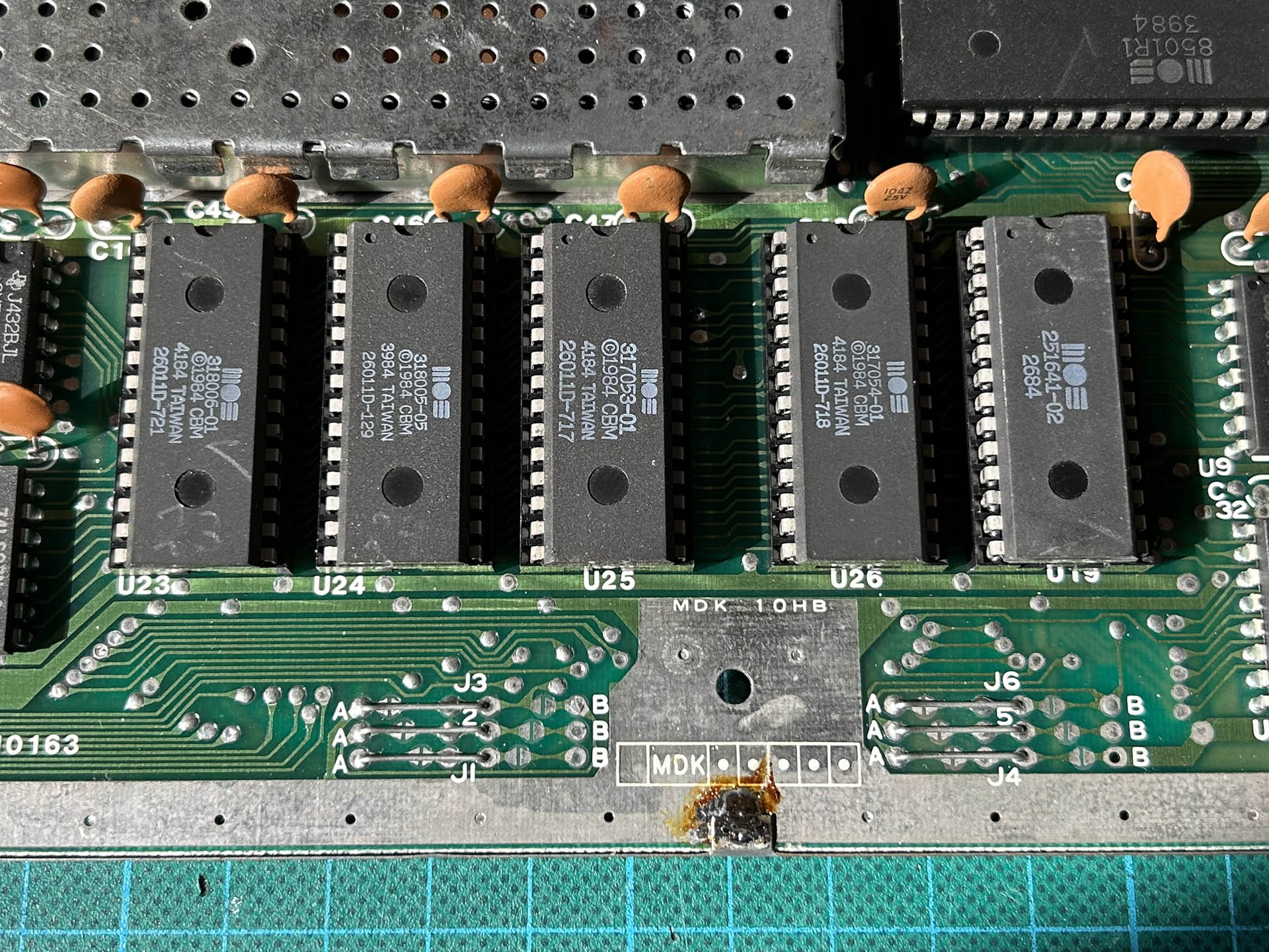
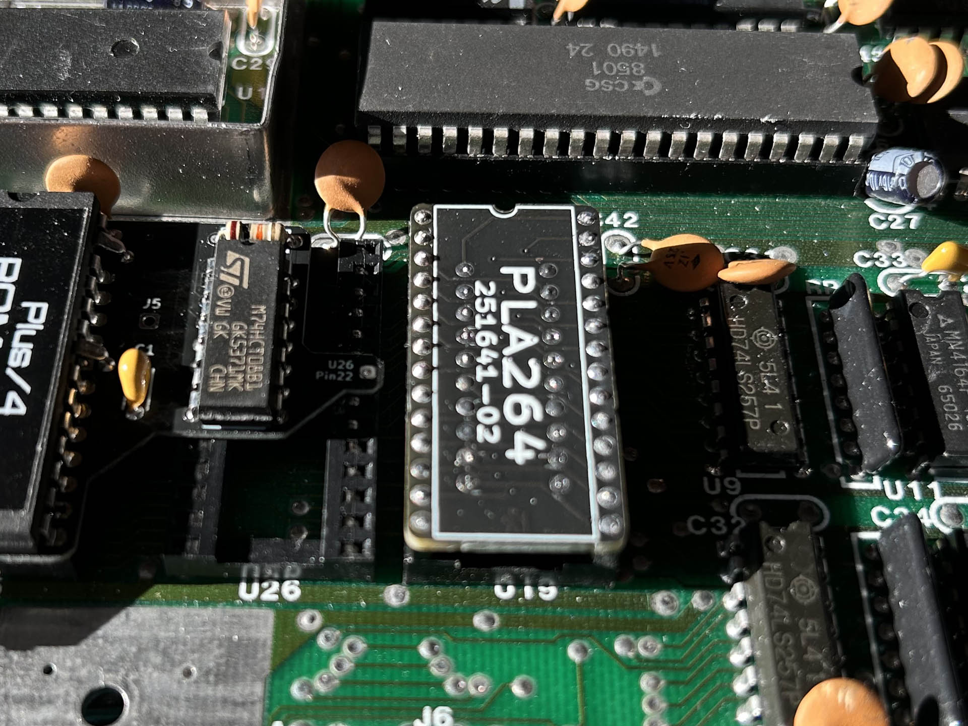
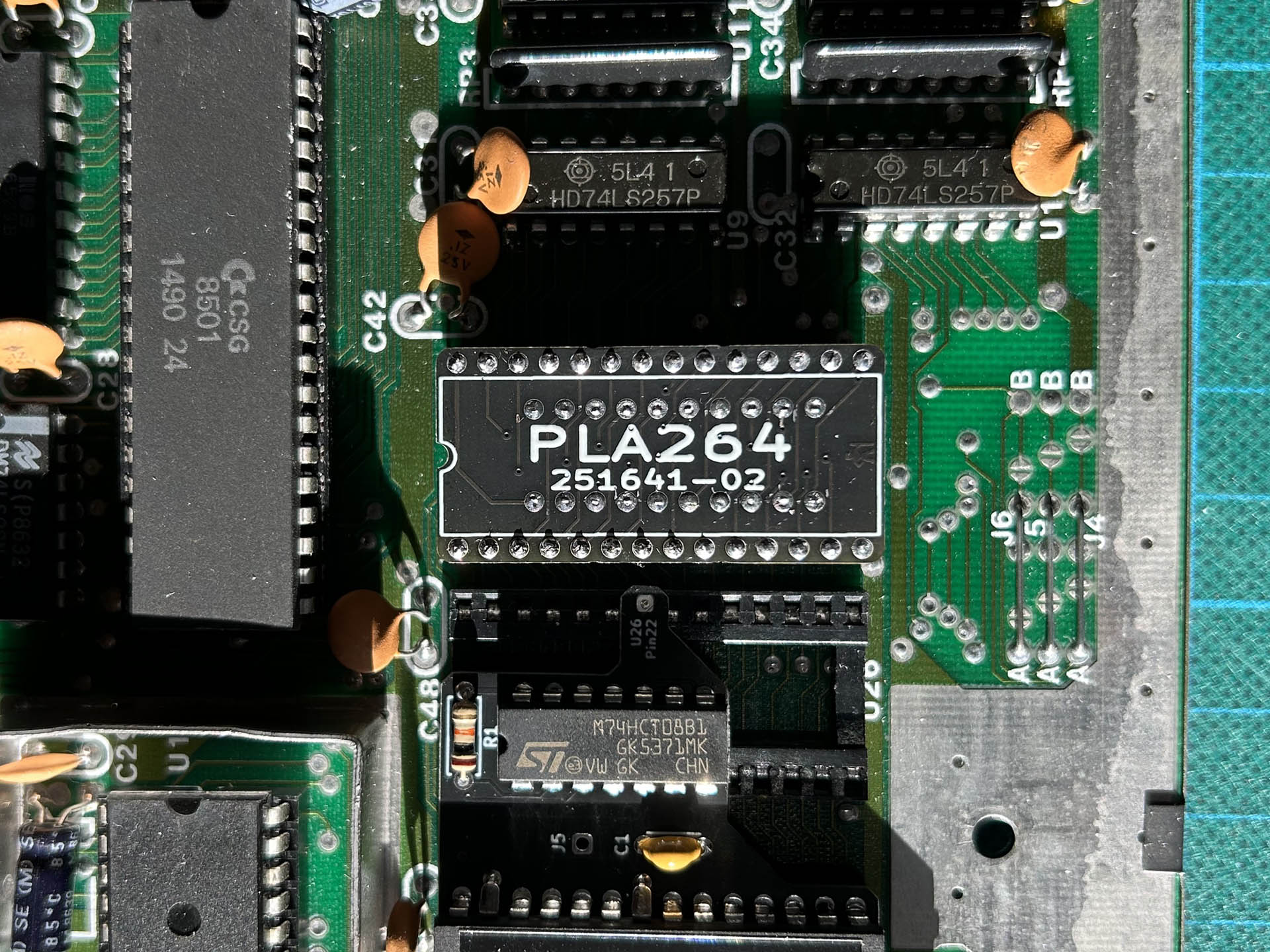
Five in a row: The four ROM chips of the Plus/4 to the left and the PLA to the right.
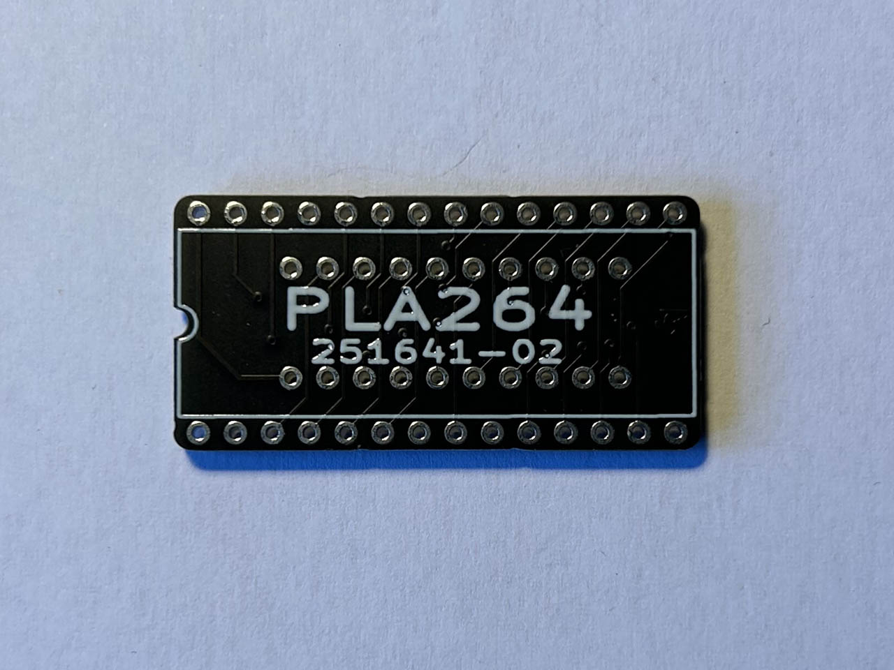
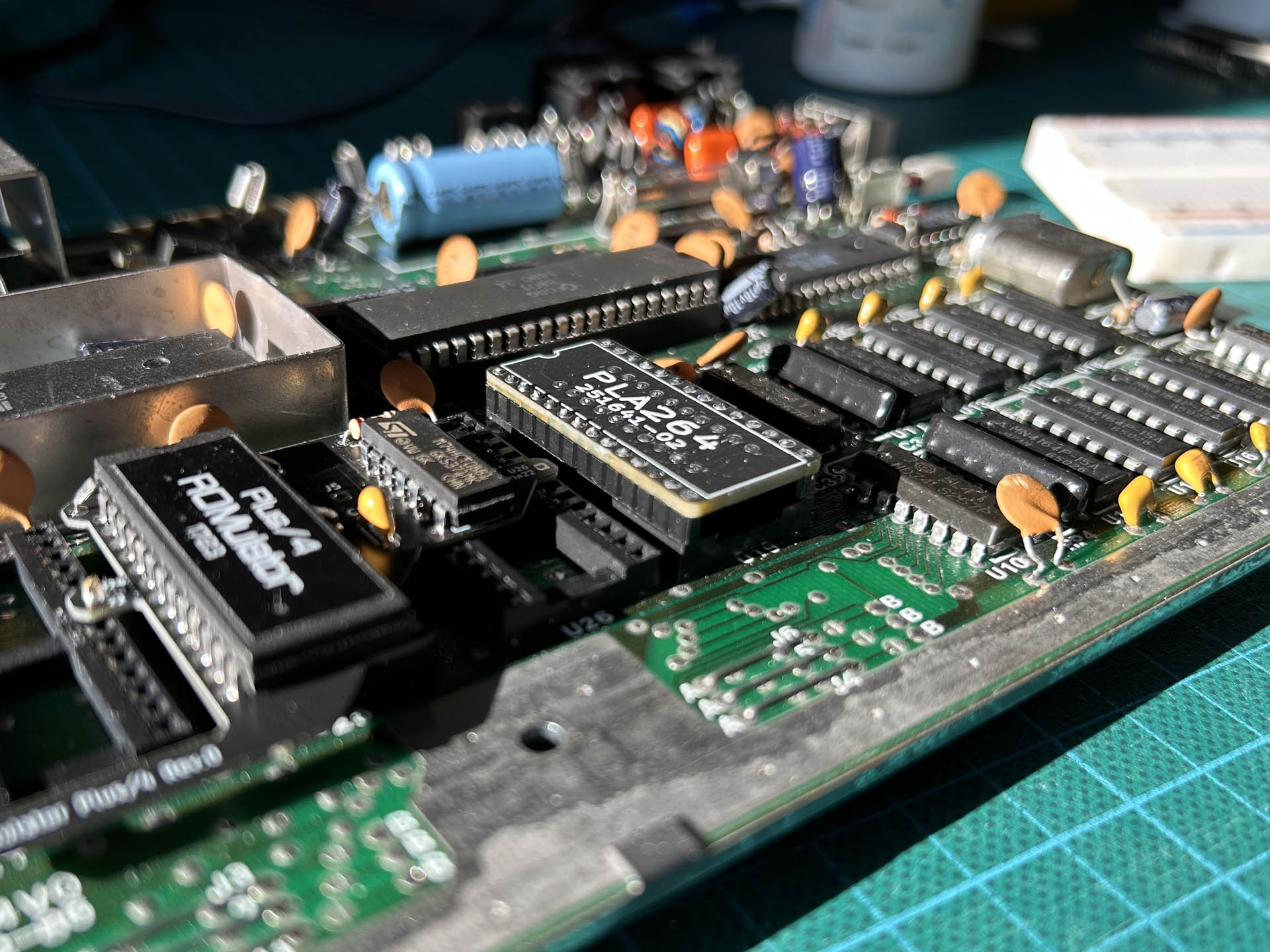
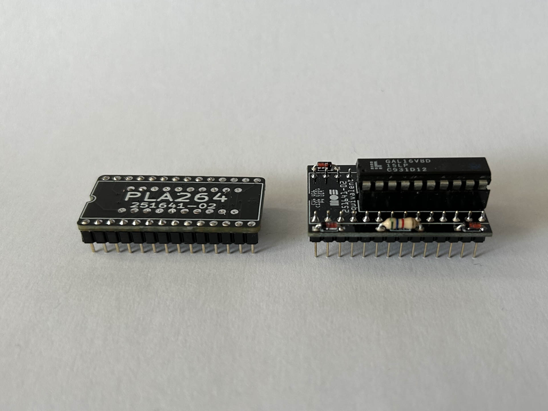
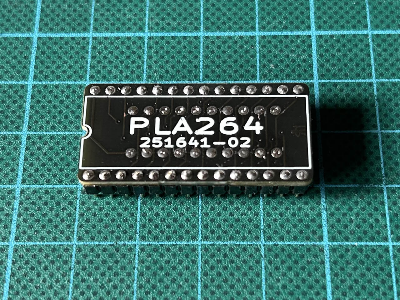
The four ROM chips of the Plus/4 are sitting all in one row, and then there is a fifth IC right next to them: the 251641-02 PLA. This PLA chip is the same for all TED based Commodore computers, the C16, the C116, and the Plus/4. In the past, I used the excellent PLA16V8 from D. Mantione as a replacement. The PLA16V8 is quick to build from cheap parts that are easily available. And for a C16 with its roomy case, it’s a perfectly adequate solution.
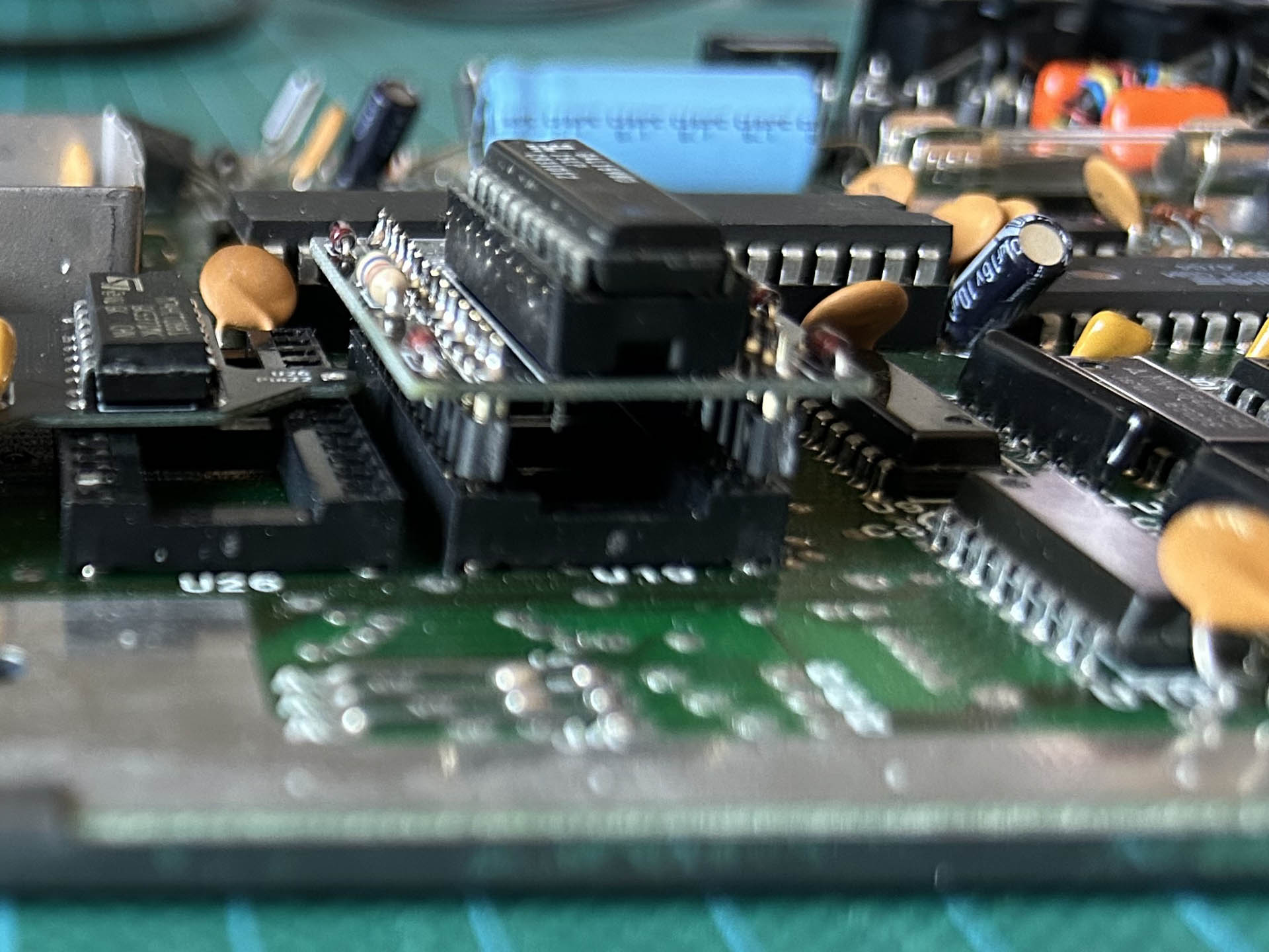
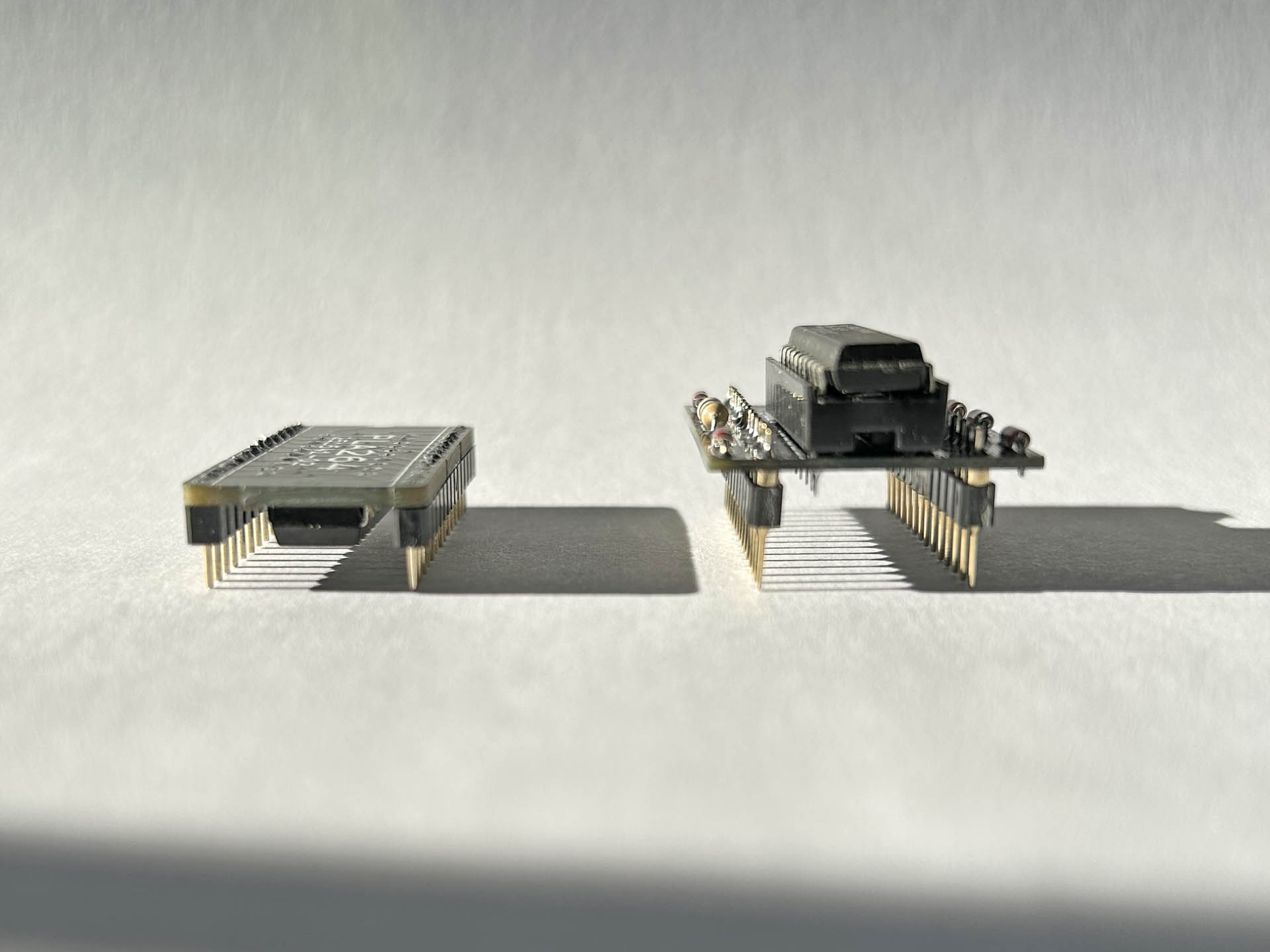
The original PLA16V18 is much too tall to fit under the keyboard of the Plus/4.
With the Plus/4, however, it’s all about space again: There are only a few millimeters between the original PLA and the keyboard above it. So while the PLA16V8 works fine on a Plus/4 motherboard, it is far too tall to fit inside the Plus/4’s case.
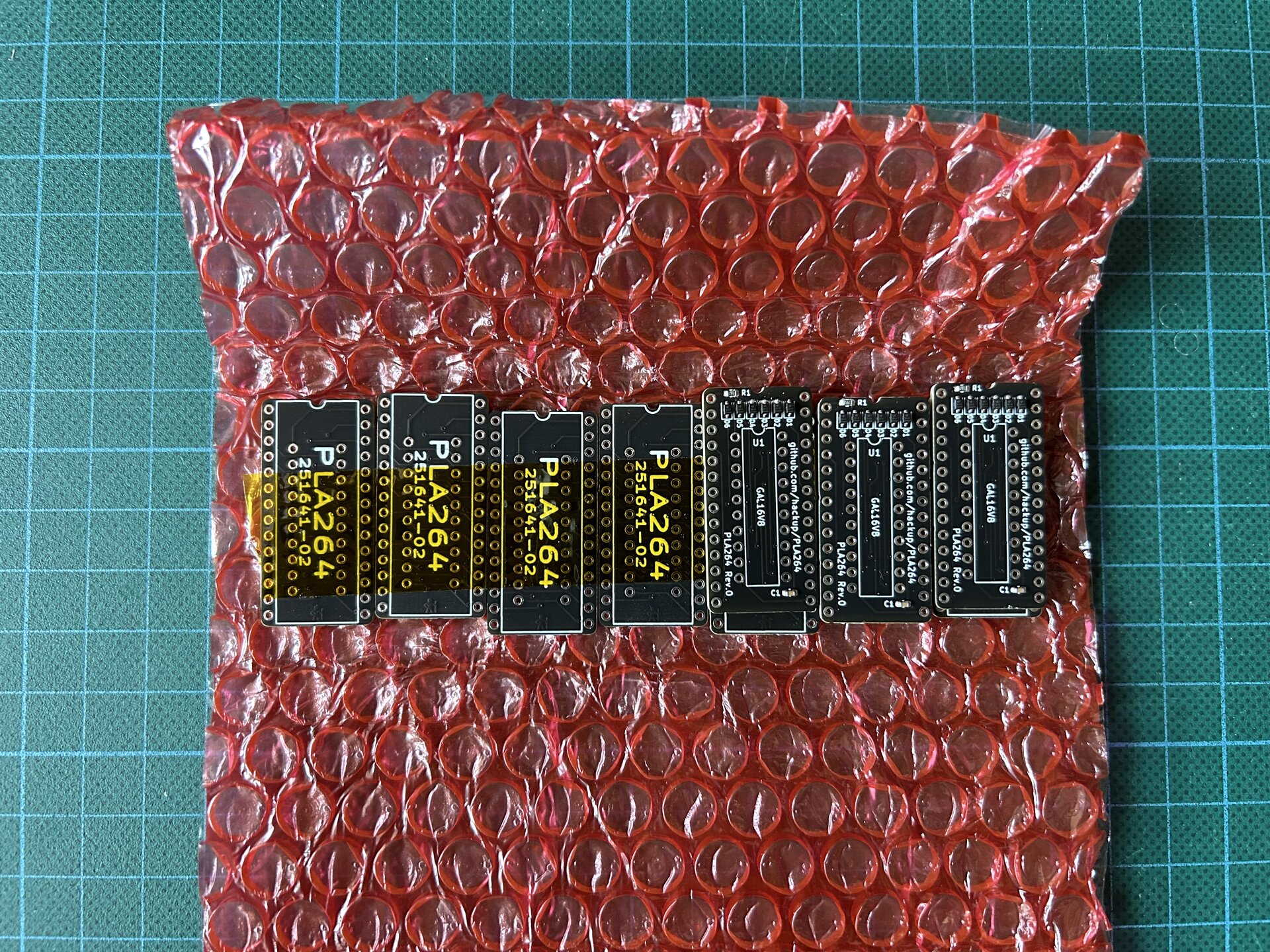
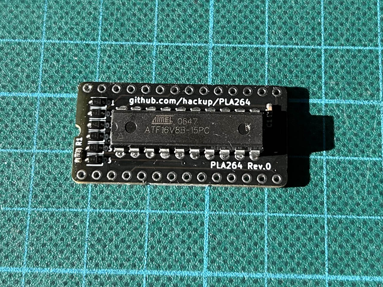
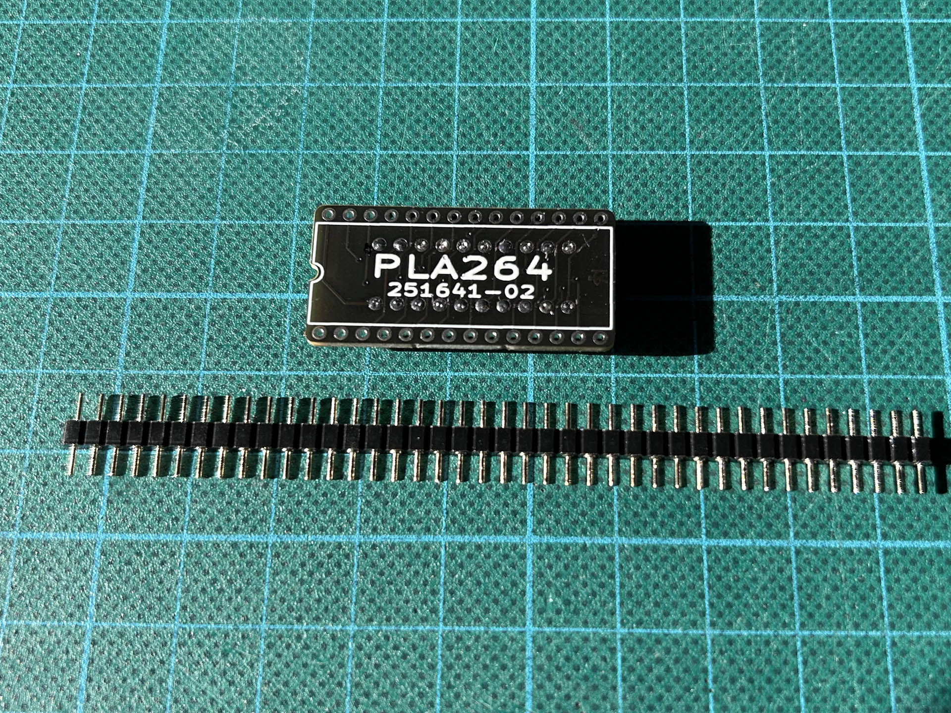
To solve this problem, I created the PLA264, an alternative PCB layout for the PLA16V8:
- I used low profile pin headers that raise the PCB only 3 mm above the IC socket.
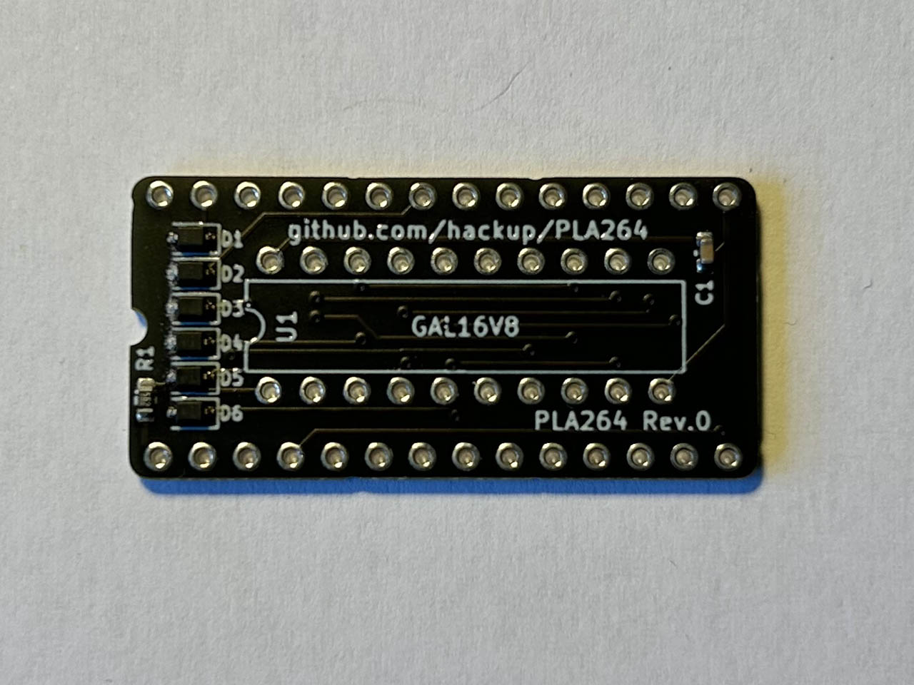
- All components are moved to the bottom side of the PCB.
- The resistor, the capacitor, and the diodes are replaced by small 0603 SMD components.
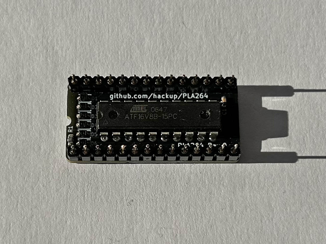
- I was able to keep the DIP package for the GAL16V8, which is easier to program.
Some PCB manufacturers will also assemble the SMD components.
Now, I can already hear some people complaining about the use of these small SMD components that are supposedly hard to solder. But (besides making the unit fit) they actually have the advantage that PCB manufacturers are able to assemble them for you if you want.
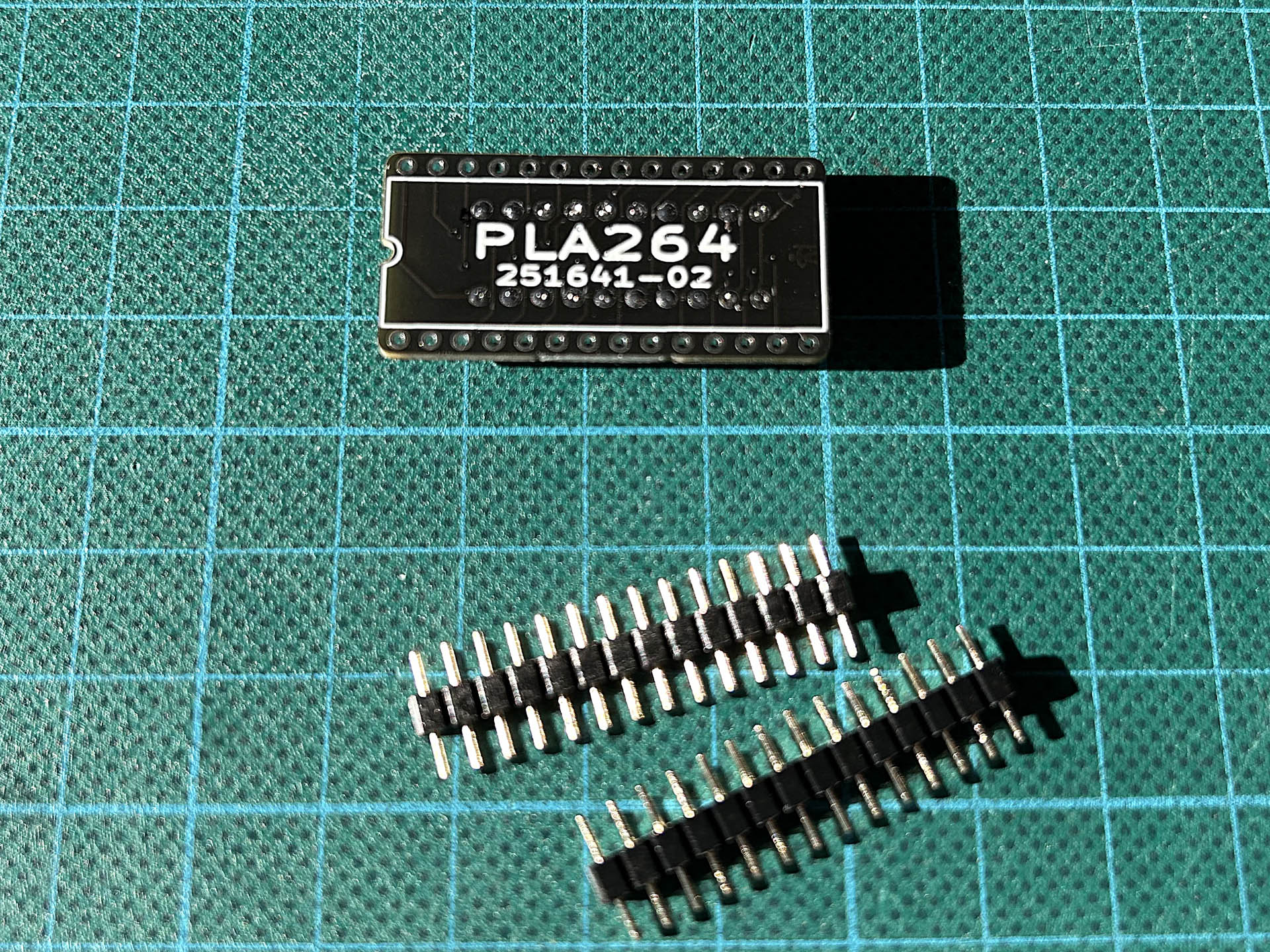
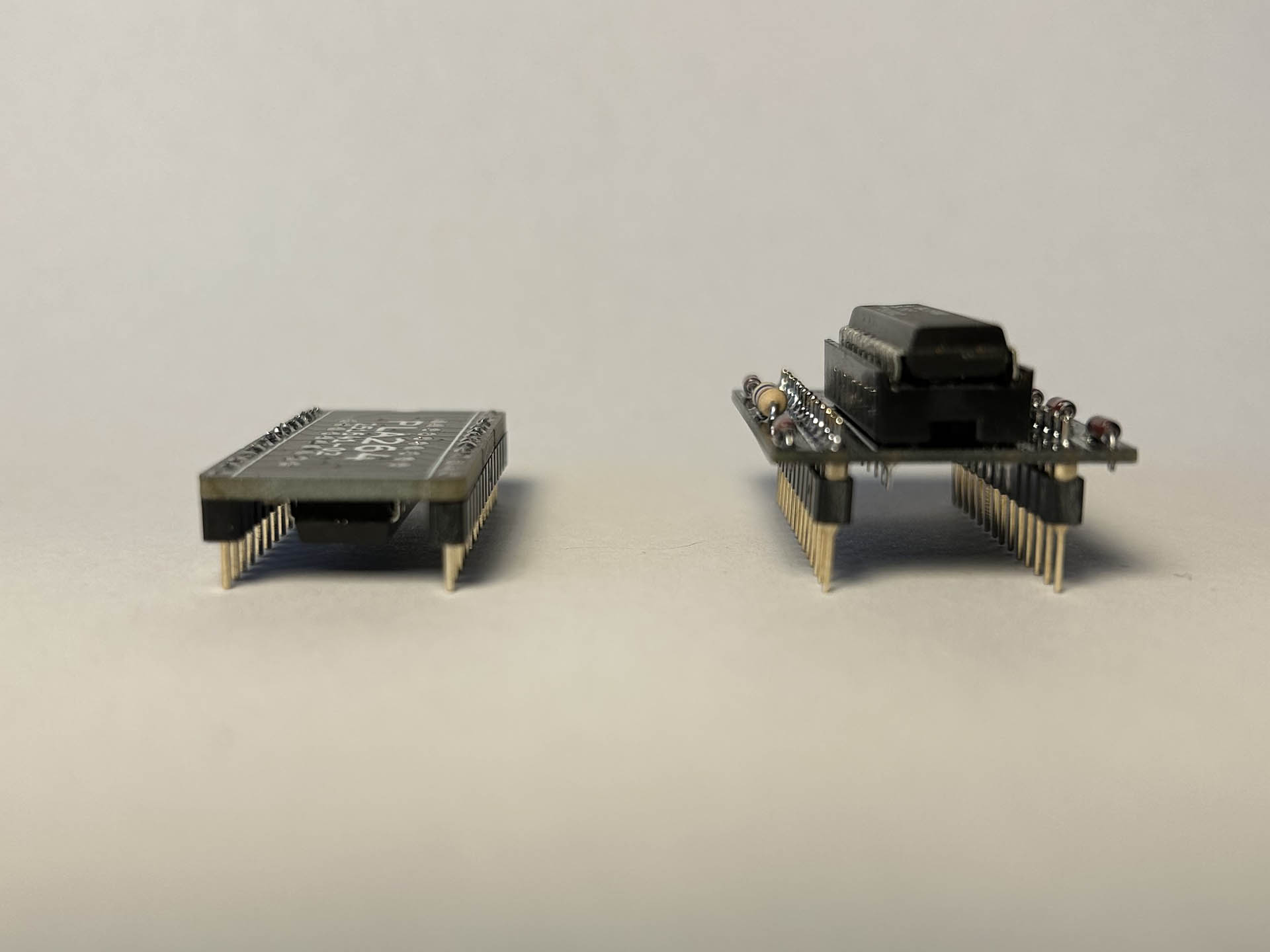
All components are located on the bottom side of the PCB.
Either way, when assembling the PCB, the SMD components should go first. Next comes the GAL16V8 (or ATF16V8). Since the PLA264 is basically a PLA16V8 with an optimized PCB layout, it uses the same JEDEC file to program the GAL. Once the GAL is programmed, it must be soldered directly to the PCB. I recommend trimming its pins before soldering so that they do not protrude from the top of the PCB. Finally, solder the low-profile pin headers, which may also need to be trimmed at the top.

The finished PLA264 next to an original PLA16V8.
Not surprisingly, initial tests of the PLA264 show that it seems to work just as well as the original PLA16V8. But now it also fits into the case of my Plus/4! A little more testing and some cleaning up is still needed. Then I will release the project files as usual.
Update 2023-05-29
For those who are interested, the project sources are now available on Github. If you just want a PCB to build the PLA264, you can order it directly from PCBWay.


Hi, do you have a spare pcb of your project to sell, I’m interest in the PLA264 and pi1541IO? I’m in Italy and I’m not confident with pcb fabs… Best regards
Pingback: Making Cartridges for the Commodore C16, C116, and Plus/4
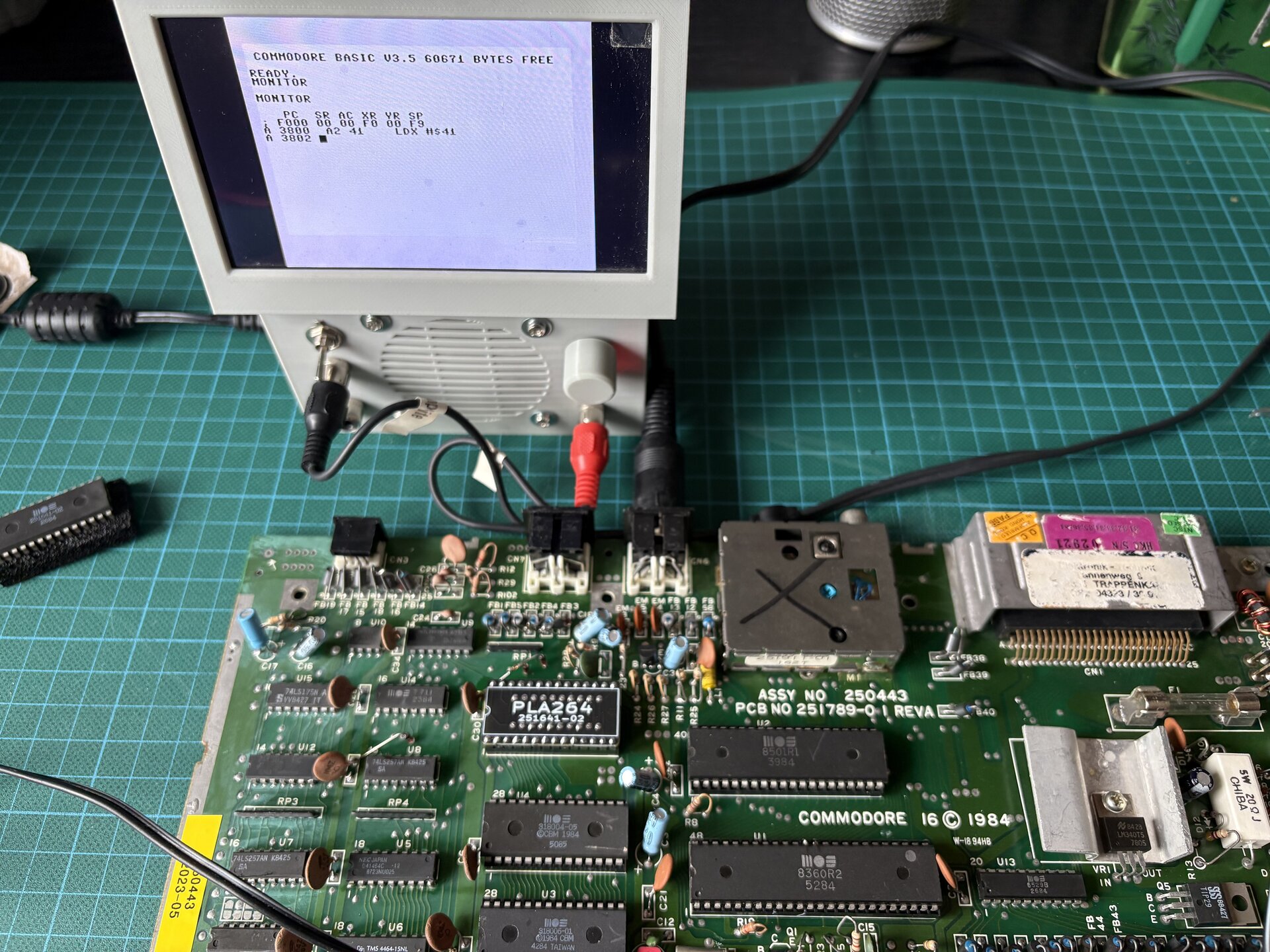
This arrangement works fine on my C16, until I come to use the built in monitor, where the assembler throws up an error.
When I try to assemble code, it just comes up with a question mark at the end of every line. For example, would turn this line
A 3800 LDX #$41
Into A 3800 LDX #$4?
And not be ready for the next instruction at 3802
All the monitor commands work ok.
After tracking down the problem to this PLA by exchanging it with a second hand one, the problem was resolved.
Thanks for the feedback. I immediately took out a C16 board to check this, because it would then most likely have affected the original, the PLA16V8. However, I cannot confirm this observation; the monitor command also works perfectly for me with the PLA264. There is probably another problem on your board that only occurs under certain conditions. Perhaps a marginal RAM chip?

Thanks for checking this. Very strange. I have no other way of checking the suspect PLA, as I only have one out of three C16/Plus4’s working.